Printed Circuit Boards (PCBs) are the foundation of modern electronics, connecting components in devices such as smartphones, medical instruments, and household appliances. As electronics have become more compact and complex, the processes used to design, build, and verify PCBs have also evolved. This has led to the development of specialized PCB lab equipment, PCB testing equipment, PCB inspection equipment, and PCB prototyping equipment.
A typical electronics lab PCB equipment setup includes tools that support every stage of development, from initial design validation to final product testing. These tools help ensure that a PCB performs correctly, safely, and consistently before it is used in real-world applications. Without proper testing and inspection, even small design errors can lead to device failure or reduced performance.
Understanding a PCB lab setup equipment list is important for students, engineers, and organizations working with electronics. It provides clarity on what tools are needed and how they contribute to reliable circuit design and production.
Importance
PCB testing and inspection play a critical role in ensuring that electronic devices function as intended. Faulty PCBs can lead to malfunctioning devices, safety hazards, or data loss. By using appropriate PCB testing equipment and PCB inspection equipment, these risks can be minimized.
For everyday users, this topic matters because nearly all modern devices rely on PCBs. Whether it is a mobile phone, a home appliance, or a vehicle control system, the reliability of these devices depends on properly tested circuit boards.
Several key challenges are addressed through proper PCB lab equipment:
- Error detection: Identifying issues such as short circuits, open connections, or incorrect component placement early in the process
- Quality control: Ensuring consistent manufacturing standards across multiple units
- Performance verification: Confirming that the PCB operates under expected conditions
- Safety assurance: Reducing risks of overheating, electrical faults, or device failure
Educational institutions and research labs also depend on electronics lab PCB equipment to teach practical skills. Students learn how to design, assemble, and troubleshoot PCBs, preparing them for roles in electronics, manufacturing, and technology development.
Recent Updates
Between 2024 and 2026, several trends have influenced PCB testing, inspection, and prototyping equipment.
One notable development is the integration of automation and artificial intelligence into PCB inspection equipment. Automated Optical Inspection (AOI) systems now use advanced image processing to detect defects more accurately and quickly than manual inspection. These systems can identify issues such as soldering defects, missing components, or alignment problems.
Another trend is the increasing use of compact and multifunctional PCB lab equipment. Modern tools often combine multiple capabilities, such as oscilloscopes with built-in signal analysis features or power supplies with programmable settings. This reduces the need for multiple standalone devices in a PCB lab setup equipment list.
PCB prototyping equipment has also evolved with the growth of rapid prototyping techniques. Desktop PCB milling machines and improved 3D printing technologies allow faster creation of prototypes without relying entirely on external manufacturing. This supports faster design iterations and experimentation.
Additionally, there is a growing emphasis on high-frequency and high-speed PCB testing. As communication technologies advance, including 5G and beyond, PCBs must handle higher data rates. This requires more precise PCB testing equipment capable of measuring signal integrity and electromagnetic behavior.
Laws or Policies
PCB testing and inspection are influenced by various standards and regulations that aim to ensure safety, quality, and environmental responsibility. In India and globally, several frameworks guide how PCBs are manufactured and tested.
The Bureau of Indian Standards (BIS) provides guidelines for electronic products, including safety requirements. These standards help ensure that devices using PCBs meet acceptable safety and performance criteria.
International standards also play a significant role. Organizations such as the International Electrotechnical Commission (IEC) and the Institute for Printed Circuits (IPC) define widely used standards for PCB design, assembly, and testing. For example:
- IPC standards: Cover aspects like soldering quality, inspection criteria, and material specifications
- IEC standards: Address electrical safety and performance requirements
Environmental regulations are another important factor. Rules related to hazardous substances, such as restrictions on lead and other materials, influence PCB design and testing processes. Compliance with such regulations ensures that electronics are safer for both users and the environment.
Laboratory setups using PCB lab equipment must also follow general electrical safety guidelines. This includes proper grounding, safe handling of high-voltage equipment, and adherence to workplace safety practices.
Tools and Resources
A well-equipped PCB lab includes a variety of tools for design, prototyping, testing, and inspection. The following table outlines common categories of electronics lab PCB equipment and their functions.
| Equipment Type | Purpose | Example Use Case |
|---|---|---|
| Oscilloscope | Visualizes electrical signals | Checking waveform integrity |
| Multimeter | Measures voltage, current, resistance | Basic circuit testing |
| Function Generator | Produces test signals | Simulating input signals |
| Power Supply | Provides controlled electrical power | Powering prototypes safely |
| Soldering Station | Assembles components onto PCBs | Manual PCB assembly |
| PCB Milling Machine | Creates prototype boards | Rapid prototyping |
| AOI System | Inspects PCB visually | Detecting soldering defects |
| X-ray Inspection System | Examines hidden connections | Inspecting multilayer boards |
| Logic Analyzer | Captures digital signals | Debugging digital circuits |
PCB Testing Equipment
PCB testing equipment is used to verify electrical performance. Common tools include multimeters for basic checks, oscilloscopes for signal analysis, and in-circuit testers that evaluate individual components on a board. These tools help identify faults before a PCB is deployed in a device.
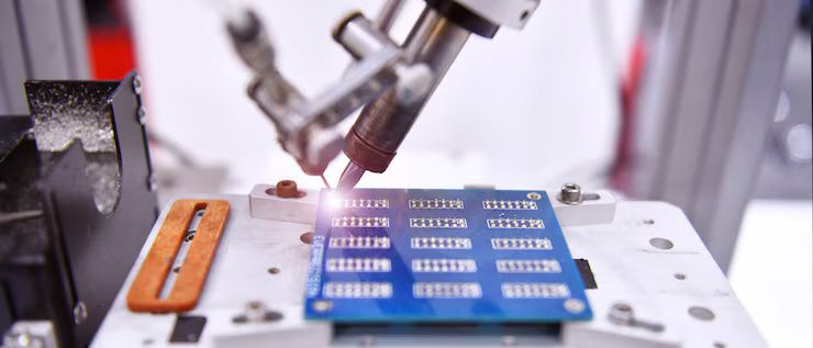
PCB Inspection Equipment
PCB inspection equipment focuses on identifying physical and visual defects. Tools such as magnification systems, AOI machines, and X-ray systems allow engineers to inspect solder joints, component placement, and internal connections.
PCB Prototyping Equipment
PCB prototyping equipment supports the creation of initial designs. Desktop milling machines, soldering tools, and design software are commonly used. These tools allow quick testing of ideas before moving to large-scale production.
Digital Tools and Platforms
In addition to physical equipment, software tools are essential:
- PCB design software: Used to create circuit layouts and schematics
- Simulation tools: Help predict circuit behavior before physical testing
- Data analysis tools: Assist in interpreting test results
Online platforms and educational resources provide tutorials, reference designs, and community support, helping users understand how to use PCB lab equipment effectively.
FAQs
What is included in a PCB lab setup equipment list?
A typical PCB lab setup equipment list includes tools such as oscilloscopes, multimeters, soldering stations, power supplies, and PCB prototyping equipment. It may also include PCB inspection equipment like microscopes or AOI systems for detailed analysis.
Why is PCB testing equipment important?
PCB testing equipment is important because it helps detect electrical faults and ensures that the circuit operates correctly. Without proper testing, issues like short circuits or incorrect signal behavior may go unnoticed.
What is the difference between PCB inspection equipment and PCB testing equipment?
PCB inspection equipment focuses on visual and physical checks, such as identifying solder defects or misaligned components. PCB testing equipment, on the other hand, evaluates electrical performance and functionality.
How does PCB prototyping equipment help in development?
PCB prototyping equipment allows engineers to create and test early versions of a circuit board. This helps identify design issues before final production, reducing errors and improving efficiency.
Can beginners use electronics lab PCB equipment?
Yes, beginners can use electronics lab PCB equipment with proper guidance. Basic tools like multimeters and soldering stations are commonly used in educational settings to teach fundamental concepts.
Conclusion
PCB testing, inspection, and prototyping equipment are essential components of modern electronics development. These tools help ensure that circuit boards are reliable, safe, and functional before they are used in devices. A structured PCB lab setup equipment list supports efficient workflows and accurate results. As technology advances, PCB lab equipment continues to evolve, enabling more precise and faster development processes. Understanding these tools provides a strong foundation for working with electronic systems.