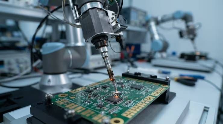
Semiconductor equipment is the collection of specialized machines and systems used to manufacture, inspect, test, assemble, and package semiconductor devices. These systems help transform raw silicon wafers into components used in computers, smartphones, vehicles, medical electronics, industrial controls, and many other technologies.
Modern semiconductor manufacturing depends on highly controlled processes. Semiconductor equipment supports activities such as wafer preparation, lithography, deposition, etching, cleaning, metrology, inspection, testing, and advanced packaging. Understanding these systems provides useful background for anyone learning about semiconductor manufacturing and microelectronics.
Context
Semiconductor manufacturing is a multi-stage process in which microscopic electronic structures are created on semiconductor wafers. A manufacturing facility, commonly called a fab, uses many specialized equipment categories because no single machine performs the complete production process.
The process generally begins with silicon wafers. Equipment prepares and cleans the wafer before successive layers of materials are deposited, patterned, etched, and inspected.
Some major semiconductor equipment categories include:
| Equipment category | Main purpose |
|---|---|
| Lithography systems | Transfer circuit patterns onto wafers |
| Deposition systems | Add controlled material layers |
| Etching systems | Remove selected material |
| Cleaning systems | Remove particles and unwanted residues |
| Metrology systems | Measure dimensions and process results |
| Inspection systems | Detect defects and irregularities |
| Ion implantation systems | Modify electrical properties of selected regions |
| Packaging equipment | Assemble and protect completed semiconductor devices |
| Test equipment | Check electrical and functional performance |
Lithography is particularly important because it defines tiny circuit features. Deposition and etching then build and shape the different layers that form electronic structures.
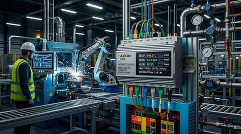
Modern facilities also rely heavily on automation, sensors, process-control software, robotics, and environmental monitoring. These technologies help maintain consistent processing conditions across large numbers of wafers.
Importance
Semiconductor equipment matters because the performance and reliability of a chip depend on precise manufacturing conditions. Very small variations in temperature, pressure, chemical concentration, particle levels, or alignment can affect a manufacturing result.
The equipment ecosystem also affects many industries beyond semiconductor manufacturing. Semiconductor devices are important components in:
- Computing and data centers
- Consumer electronics
- Automotive systems
- Telecommunications
- Industrial automation
- Medical electronics
- Aerospace and space systems
- Renewable-energy equipment
Advanced semiconductor manufacturing requires equipment capable of controlling increasingly small structures. At the same time, mature semiconductor processes remain important for many applications, including power electronics, sensors, automotive components, and industrial devices.
Equipment is therefore connected to the broader semiconductor supply chain, which includes materials, chemicals, components, software, manufacturing facilities, packaging, and testing.
Recent Updates
Semiconductor equipment development is increasingly influenced by artificial intelligence, high-performance computing, advanced packaging, and the growing complexity of electronic systems.
SEMI's 2025 market outlook projected test equipment growth of about 23% in 2025 and a further 5% increase in 2026. Its forecast also projected assembly and packaging equipment growth of 15% in 2026, reflecting increased interest in advanced packaging for AI and high-performance computing applications.
Advanced packaging is becoming an important part of semiconductor system design. Technologies such as chiplets and 2.5D and 3D integration can combine multiple semiconductor components within sophisticated packages. The European Commission's 2026 advanced-chip initiative includes a proposed semiconductor facility combining advanced manufacturing with chiplet integration and 2.5D/3D packaging.
Automation is another major development. Semiconductor equipment increasingly incorporates sensors, automated material handling, process monitoring, and data analysis. These capabilities can help manufacturers identify process variation and maintain tighter production controls.
Environmental considerations are also receiving greater attention. The U.S. Environmental Protection Agency notes that semiconductor manufacturing uses fluorinated greenhouse gases in processes such as plasma etching and chemical vapor deposition chamber cleaning. Manufacturers have investigated process improvements, alternative chemicals, and destruction technologies to reduce emissions.
Laws or Policies
Semiconductor manufacturing is affected by several types of laws and government policies. Requirements vary according to the country, facility, chemicals, equipment, and manufacturing activities involved.
In the United States, semiconductor manufacturing facilities are subject to environmental requirements addressing hazardous air pollutants. EPA's semiconductor manufacturing NESHAP framework covers activities ranging from crystal growth and wafer fabrication through testing and assembly.
Chemical regulation is another consideration. EPA amended its Toxic Substances Control Act rules in December 2024 concerning the review of new chemicals, including certain PFAS and other persistent, bioaccumulative, and toxic substances.
EPA also reported in 2026 that one additional PFAS was added to the U.S. Toxics Release Inventory beginning with reporting year 2026, bringing the number of PFAS subject to TRI reporting to 206.
Government semiconductor policies can also focus on manufacturing capacity and technology development. In Europe, the European Chips Act supports semiconductor research, manufacturing, and packaging, with the broader objective of strengthening the region's semiconductor ecosystem.
In June 2026, the European Commission announced a technology sovereignty package that included a proposed Chips Act 2.0 focused on semiconductor capacity, supply resilience, and advanced technologies.
These examples show why semiconductor equipment planning must consider both technical requirements and applicable regulatory frameworks.
Tools and Resources
People learning about semiconductor equipment can use several reliable resources to understand manufacturing systems and industry developments.
Useful resources include:
- SEMI publications for semiconductor equipment and manufacturing market information.
- U.S. EPA resources for environmental requirements and semiconductor manufacturing emissions.
- European Commission semiconductor pages for information about the European Chips Act and related initiatives.
- Equipment manufacturer technical documentation for understanding individual process categories.
- Semiconductor textbooks and university materials for fundamentals of wafer fabrication.
- Process simulation and engineering software for studying manufacturing concepts.
When researching a particular machine, it is useful to examine its process function, wafer size compatibility, material requirements, operating conditions, automation features, inspection capabilities, and applicable environmental requirements.
FAQs
What is semiconductor equipment?
Semiconductor equipment refers to specialized machines used throughout chip manufacturing, including wafer processing, lithography, deposition, etching, cleaning, inspection, testing, and packaging.
Why is lithography equipment important?
Lithography equipment transfers microscopic circuit patterns onto semiconductor wafers. Pattern accuracy is essential because these structures form the basis of many electronic components.
What does semiconductor metrology equipment do?
Metrology equipment measures characteristics such as dimensions, thickness, alignment, and other process parameters. This information helps manufacturers evaluate whether processes are producing the intended results.
Is semiconductor equipment used only for advanced chips?
No. Equipment is used for both advanced and mature semiconductor processes. Different applications can require different manufacturing technologies, materials, wafer sizes, and process conditions.
Why is advanced packaging becoming important?
Advanced packaging can integrate multiple semiconductor components within a single package. Chiplets and 2.5D/3D approaches are being investigated for applications requiring greater system performance and integration.
Conclusion
Semiconductor equipment forms the technological foundation of modern chip manufacturing. Different equipment categories perform specialized tasks, from wafer preparation and pattern formation to inspection, testing, and packaging.
Recent developments show increasing attention to advanced packaging, automation, AI-related computing requirements, process monitoring, and environmental considerations. Government policies in major semiconductor regions are also influencing manufacturing capacity and technology development.
Understanding semiconductor equipment begins with learning the role of each process and how individual systems work together. As semiconductor structures and packages become more sophisticated, equipment remains an important part of the broader microelectronics ecosystem.
For beginners, studying the manufacturing sequence from wafer preparation through final testing provides a practical way to understand how semiconductor manufacturing systems operate and why each equipment category has a specific role.